Output Ripple Measurement Methods for DC-DC Converters II
Roland van Roy | AN079
Output voltage ripple is an important parameter of power converters. Some loads are quite sensitive to supply voltage ripple, and some Core rails specify a tight supply voltage tolerance band that must be met, including static tolerance, supply voltage ripple, and load transient over- and undershoot. Accurate ripple measurement can be tricky, especially with high frequency switch-mode power converters. This design tip document will introduce some practical methods for output ripple voltage measurement.
1 Introduction
Modern electronic applications usually contain embedded computing and wireless connectivity functions, and these circuits often have high pulsating and heavy loading behaviors, while requiring low input voltage ripple. The new generations of DC-DC converters will therefore be required to have fast transient response to maintain stable output voltage under the fast fluctuating load conditions, and their output ripple should be small to avoid deteriorating the performance of sensitive circuits. Accurately measuring power converter output ripple can be a challenge. This document explains DC-DC converter output ripple and provides several tips how to get more accurate measurement results.
Important considerations are listed below:
- Ripple voltages are small, and the measurement equipment must have sufficient sensitivity, which sometimes requires special probes. An oscilloscope is normally used for measuring supply voltage ripple.
- Ripple measurements are always specified over a certain bandwidth. 20MHz bandwidth is most commonly used, but some applications may require a higher measurement bandwidth like 200MHz.
- The load on the supply can have a big impact on the measured ripple. This is especially important for power supplies that operate in pulse skip or Eco mode during light load conditions. In addition, dynamic load changes during the ripple measurement can increase the measured ripple value.
- The measurement environment can easily influence the measured value, especially when measuring with high bandwidth settings near high frequency switching signals. Also nearby equipment or even the measurement equipment itself can generate noise into the ripple measurement, which should not be mistaken for DUT generated noise.
2 Tip 1: Check your equipment and environment
noise
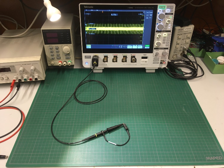
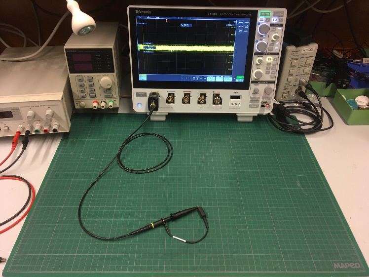
Before doing ripple measurements, it is always good to do an environment check: Connect the measurement probe tip to the probe ground lead and place it on the lab table as shown in the Figure 1 below: Set the scope to maximum bandwidth, with sufficient sample rate.
|
Ambient noise measurement with LED light switched on
|
Ambient noise measurement with LED light switched off
|
|
|
|
|
|
|
|
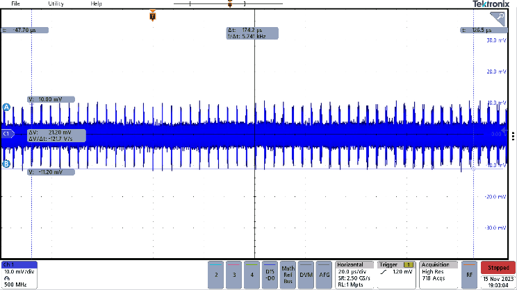
Measurement with LED light on shows 21mVpp with switching noise (10:1 probe, 500MHz bandwidth)
|
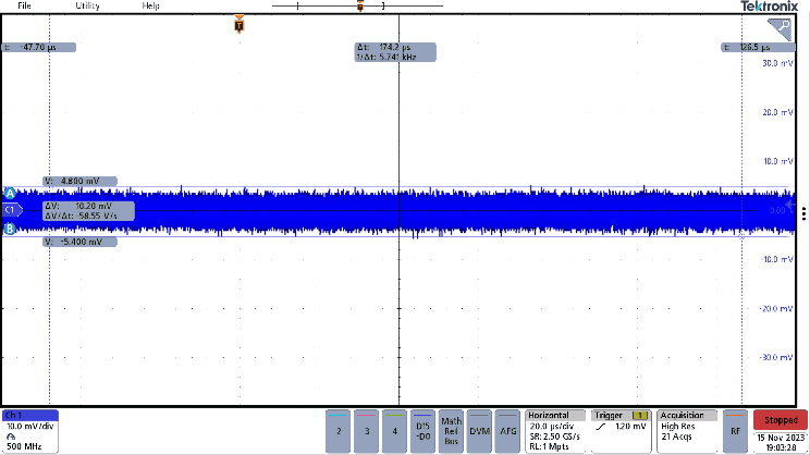
After switching off the LED lamp, the noise is reduced to 10mVpp (10:1 probe, 500MHz bandwidth)
|
Figure 1
From the above measurement example, it can be seen that a simple 10:1 probe with ground loop at high bandwidth setting (500MHz) can easily pick-up noise from the environment. Make sure that noisy equipment is switched off when doing ripple measurements.
3 Tip 2: Know what kind of ripple
signal could be expected
Knowing what to expect is also helpful when doing ripple measurements, so it is a good idea to do some ripple calculations or simulations before hooking up the scope to your board.
3.1 Continuous Conduction Mode (CCM) output ripple
For Buck converters (Figure 2), the output ripple across the output capacitor in continuous conduction (CCM) mode is caused by the inductor ripple current flowing through the output capacitor. Since the capacitor voltage is the integral of the capacitor current, and the Inductor ripple current in CCM is a triangle waveform, the pure capacitor ripple voltage in CCM consists of a positive and negative parabola voltage as shown in below Figure 3.
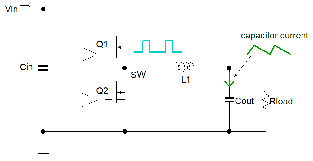
Figure 2
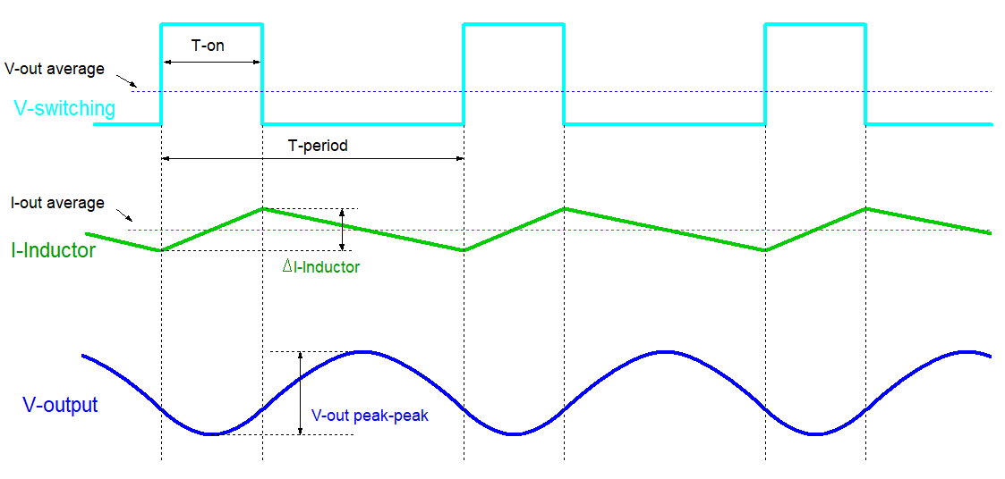
Figure 3
The inductor ripple current DIL can be found from: 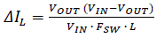
The output capacitor ripple voltage can be found from: 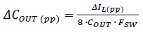 which is valid for low ESR MLCC capacitors.
In case the output capacitor has some ESR, the ripple voltage will be increased with: 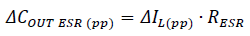
In case of MLCC capacitors, be sure to use the effective capacitance including DC bias when making these calculations.
From the formula’s, it can be seen that the load current is not present. It means that buck converter output ripple voltage does not change when load current is changed, as long as the converter stays in CCM mode.
3.2 Pulse Skip Mode (PSM) output ripple
Richtek’s Buck converter series often have a version that operates in PSM mode in light load conditions.
When the load current reduces, at a certain point, the inductor ripple current valley will reach zero. Parts with PSM mode will then start to work in Diode Emulation Mode, which means that the low-side MOSFET will only be on the positive part of the inductor current. During the time where the inductor would be negative, both high-side and low-side MOSFETs will be off, and the switching waveform will show some damped ringing, which is caused by the resonance of the inductor and parasitic capacitance at the switch node. The converter will stay in this low Iq sleep mode while the output voltage is discharged by the load. A new ON time will be generated once the feedback voltage reaches the PSM voltage reference threshold. (Figure 4)
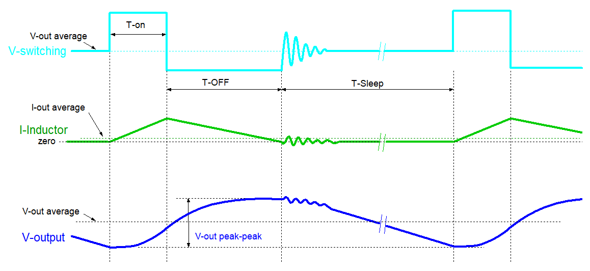
Figure 4
In light load operation, the output voltage will thus be charged by the positive triangle current during TON and TOFF, and slowly discharged by the load current during the TSLEEP time where both MOSFETs are off.
The output voltage ripple during PSM mode can be estimated by: 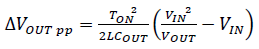
For ACOT® converters, the ON time in PSM mode is similar to the ON time in CCM mode: 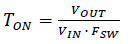
Current mode converters often set a certain peak inductor current during PSM: 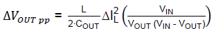
PSM output ripple amplitude is depending on load current: When load increases, the ripple amplitude will reduce, as the load current also discharges the capacitor during the TON +TOFF period. Above formulas are valid for very light (practically zero) load and single ON time PSM operation.
4 Tip
3: Understand parasitic effects
Converter output ripple can be influenced by component parasitic parameters, especially at higher switching frequencies.
The output capacitor ESR will add a triangle voltage to the output ripple. MLCC capacitors have very low ESR, around 3~5mΩ.
Polymer output capacitors have higher ESR, often ranging from 10~50mΩ. For these types, the triangle waveform in the output ripple will be more pronounced.
Output capacitors also have parasitic series inductance ESL. For MLCC types, the ESL is rather small, 0.2~0.4nH, but polymer capacitors have higher ESL around 1~2nH. In Buck converters, the ESL will add a square wave to the total voltage. The effect of the different capacitor parasitic parameters is shown in Figure 5.
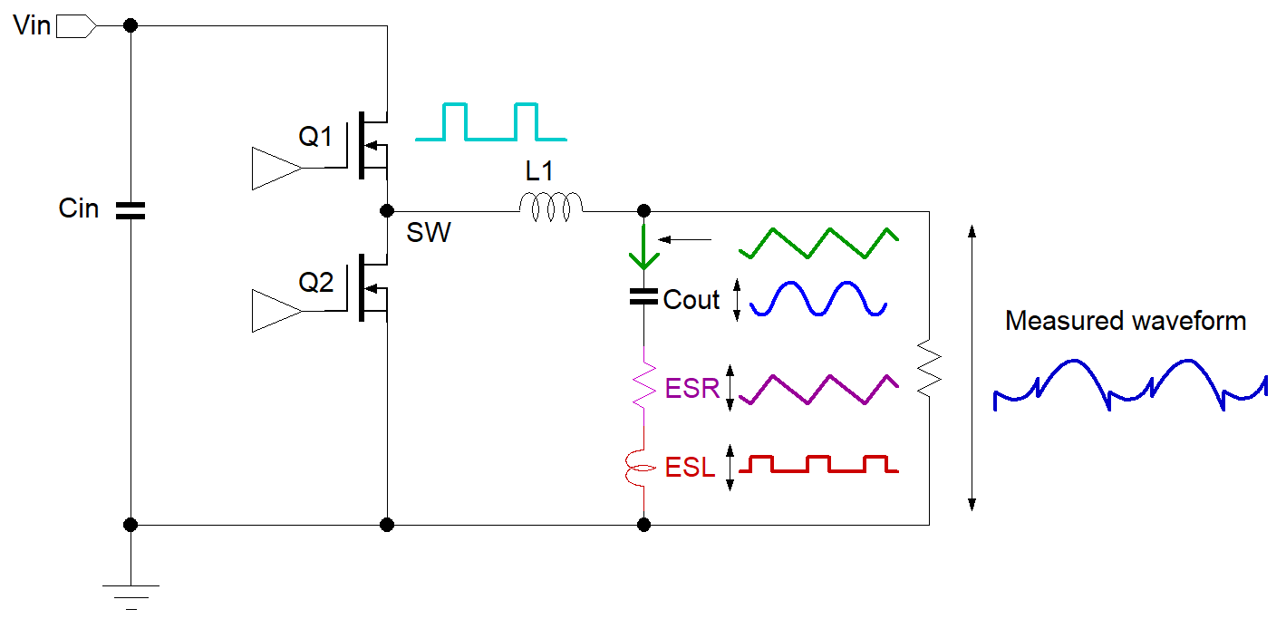
Figure 5
Inductors have parasitic parallel capacitance, ranging from a few pF to 10~15pF depending on structure, size and rating.
The inductor parallel capacitance will transfer some of the fast edges of the switching waveform to the output, resulting in high frequency spikes in measured waveform (Figure 6). You need to set the scope to high bandwidth to see these spikes.
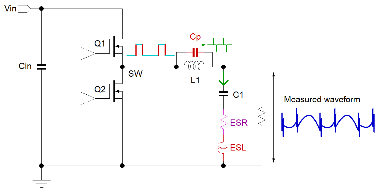
Figure 6
5 Tip
4: Noise sources in switching converters that can influence ripple measurement
Output ripple is normally small, so the oscilloscope needs to be set to high voltage sensitivity. This setting is easily influenced by power supply generated noise. One of the most common noise sources is the stray magnetic field from the inductor. Many of the popular cheap inductors are semi-shielded I cores with ferrite powder epoxy around the windings. These still generate considerable stray magnetic field. Any nearby loop will pick-up some the stray-magnetic field and the loop inductance will produce a small square-wave voltage across the loop ends.
Figure 7 shows a compact size Buck converter board with a semi-shielded coil, and the oscilloscope probe with relatively large ground lead loop. This loop may pick-up inductor stray magnetic field, which can superimpose a square wave into the output voltage ripple measurement.
Figure 7
Figure 8 (red waveforms) show the possible output ripple waveforms when the measurement is influenced by stray magnetic field: It can be seen that the switching converter square-wave is super imposed upon the ripple voltage. The super imposed waveform polarity depends on the inductor orientation and the pick-up loop orientation.
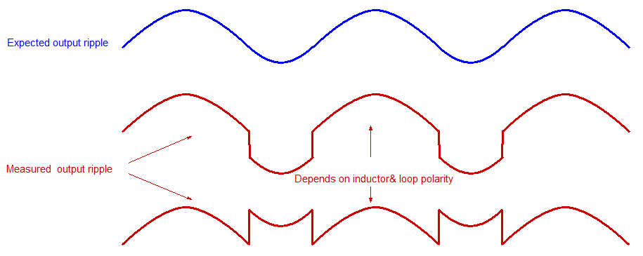
Figure 8
In the bottom red waveform, the voltage step in the waveform could be caused either by the output capacitor ESL, or the field radiation into the measurement loop of the probe tip and ground. This can be checked by moving the probe: If the amplitude of the super-imposed square wave changes when moving the probe loop in different directions, the noise is coming from probe loop stray field pick-up. This is why it is important to minimize the probe tip to probe ground loop when measuring close to inductors. Another way to check is to reverse the inductor orientation on the PCB: if the super imposed waveform polarity reverses, the voltage step in the ripple waveform is also coming from probe loop stray field pick-up.
Figure 9 shows a better way to measure output ripple:
The long ground lead is replaced by the short spring around the probe tip ground ring. This significantly reduces the area of the ground loop and reduces stray field pick-up.
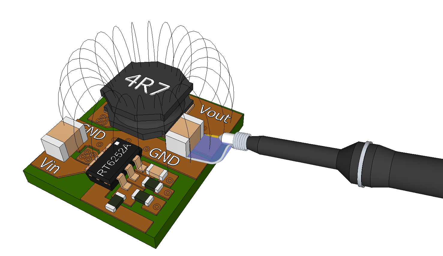
Figure 9
However, in some cases, even this smaller loop will still pick-up stray-field, especially in high frequency converters, and when the measurement point is very close to the inductor. For these cases, it is better to use a short piece of twisted wire with very short loop area at the output capacitor side, and connect the probe some distance away from the inductor, as shown in Figure 10. The twisted wire method also makes it easier to connect the fragile probe tip to the measurement point. IC socked pins can be used for this.
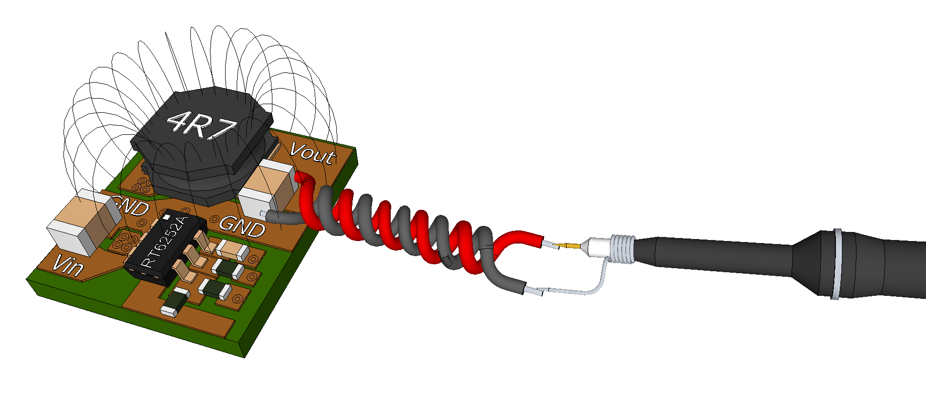
Figure 10
6 Tip 5: Low noise switching
signal measurement
It may sometimes be desirable to measure the switching waveform together with the output ripple voltage, for example to trigger the scope on the switching waveform. When connecting the 2nd probe to the switching signal directly as shown in Figure 11, you’ll find that this connection adds a lot of switching noise to the output ripple voltage measurement.
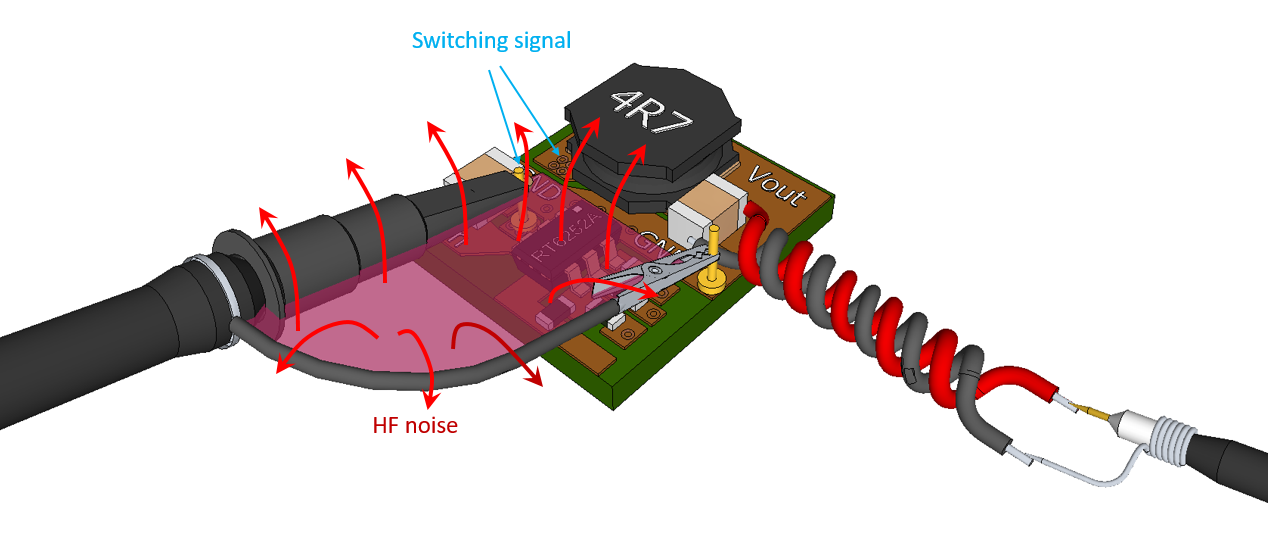
Figure 11
This extra switching noise in the ripple measurement is caused by the probe capacitance of the CH2 probe that is measuring the switching waveform: The fast rise and fall times of the switching signal result in HF current pulses into the long CH2 probe wires. This HF current causes a lot of HF radiation, and this HF noise will find its way into the output voltage ripple measurement.
You can try to use very short ground wire for the CH2 probe connection to the switching signal, but an easier way to solve this is to minimize the HF current in the CH2 probe. A useful switching signal can also be picked-up by placing the CH2 probe close to the switching signal instead of directly connecting it to the switching signal. In this case, the HF current in the CH2 probe is minimal, and the CH1 ripple measurement is not influenced. Of course, you will lose the DC information from the switching signal, but for triggering the scope on the switching waveform capacitive pick-up will work well. An easy way to get a stable switching signal capacitive pick-up is by soldering a piece of isolated wire to the switching signal, pulling out the isolation partly from the wire and clamp the probe to the top part of the isolation. The probe clamp distance to the wire inner lead will determine the amount of capacitive pick-up. See Figure 12.
Figure 12
7 Practical example 1: RT6252A
ACOT® Buck converter in 12V to 5V, 2A small size application
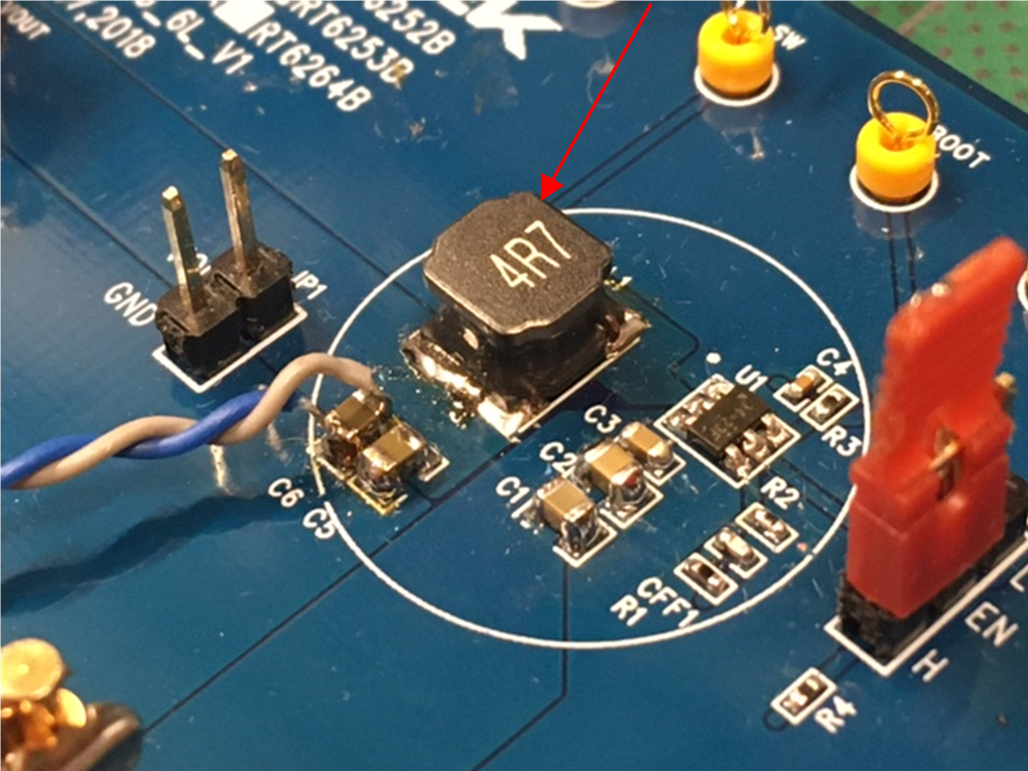
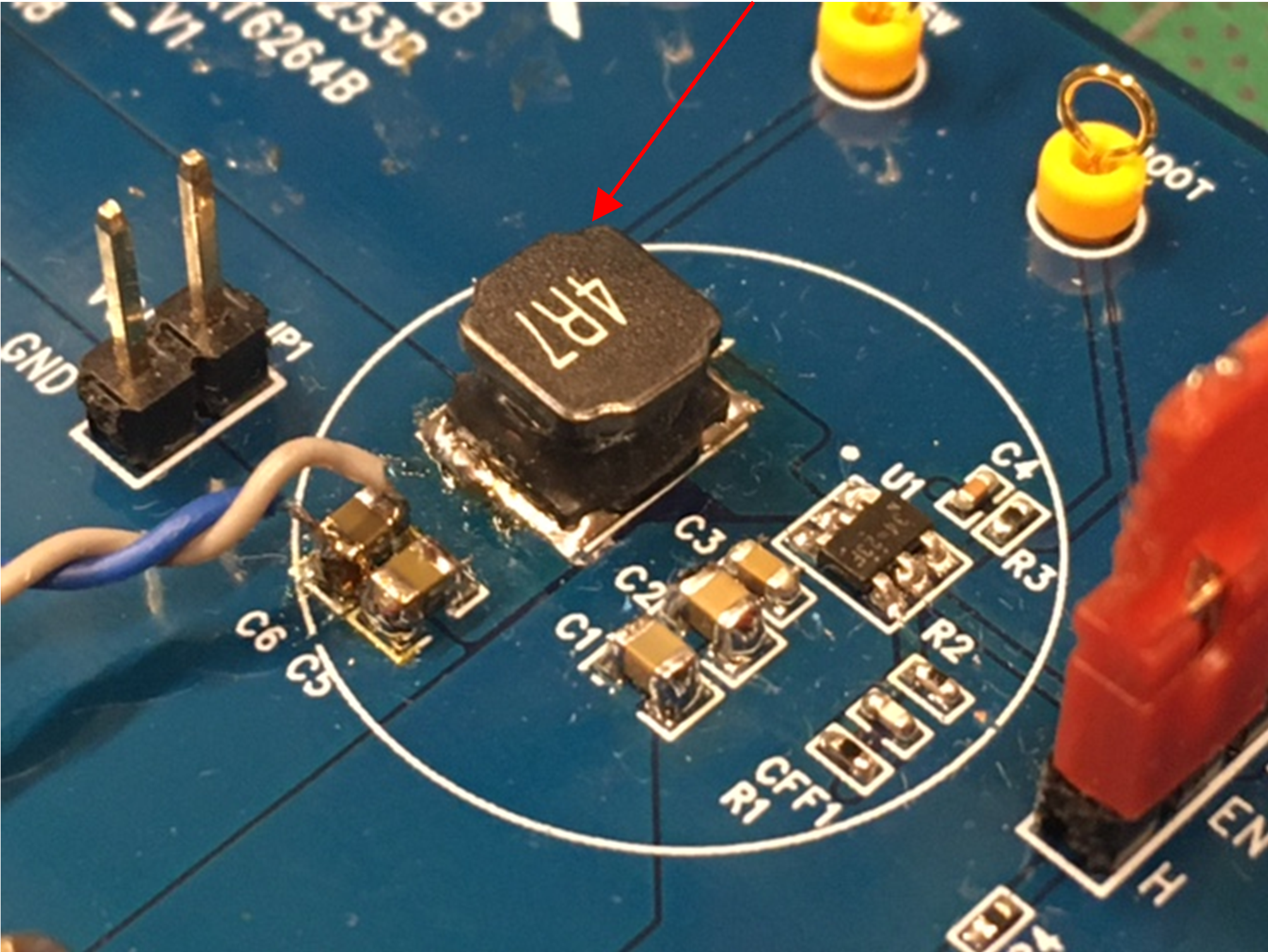
The RT6252A is a cost effective 17V rated 3rd generation ACOT® buck converter with 2A output current capability and automatic PSM mode at light load. The converter runs at 580kHz in CCM mode. The EVB schematic and layout is shown in Figure 13.
Figure 13
The two 22μF/6.3V 0805 MLCC output capacitors drop to 8μF at 5V DC bias, and at low AC voltage ripple, may drop another 30%. Each capacitor has 3mΩ ESR and around 0.2nH ESL (see Figure 14). For this application calculation, we use 14μF total capacitance, 1.5mΩ total ESR and 0.1nH total ESL.
Figure 14
The inductor MNR5040-4R7 has a self-resonance of 43MHz, therefore C-parallel = 2.9pF.
The inductor ripple current 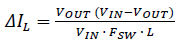 = 1.1App
The output capacitor CCM ripple voltage = 17mVpp
The 1.5mΩ ESR adds 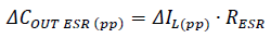 = 1.7mVpp, so total CCM ripple is 18.7mVpp
For the high frequency behavior with parasitic components, a simple LTSpice simulation shows the below results: (Figure 15)
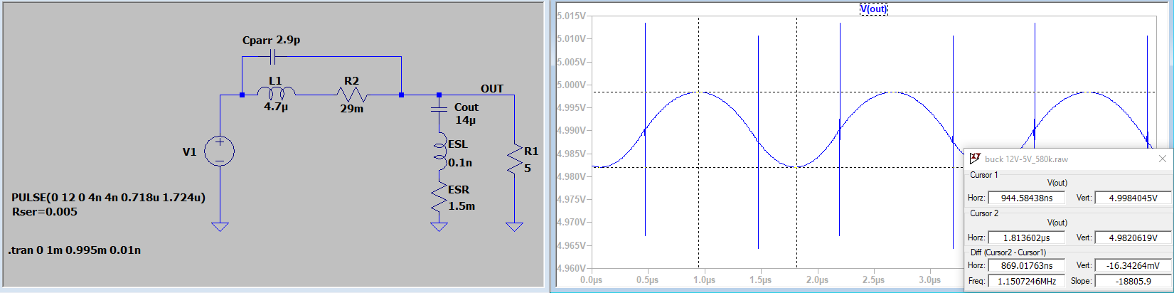
Figure 15
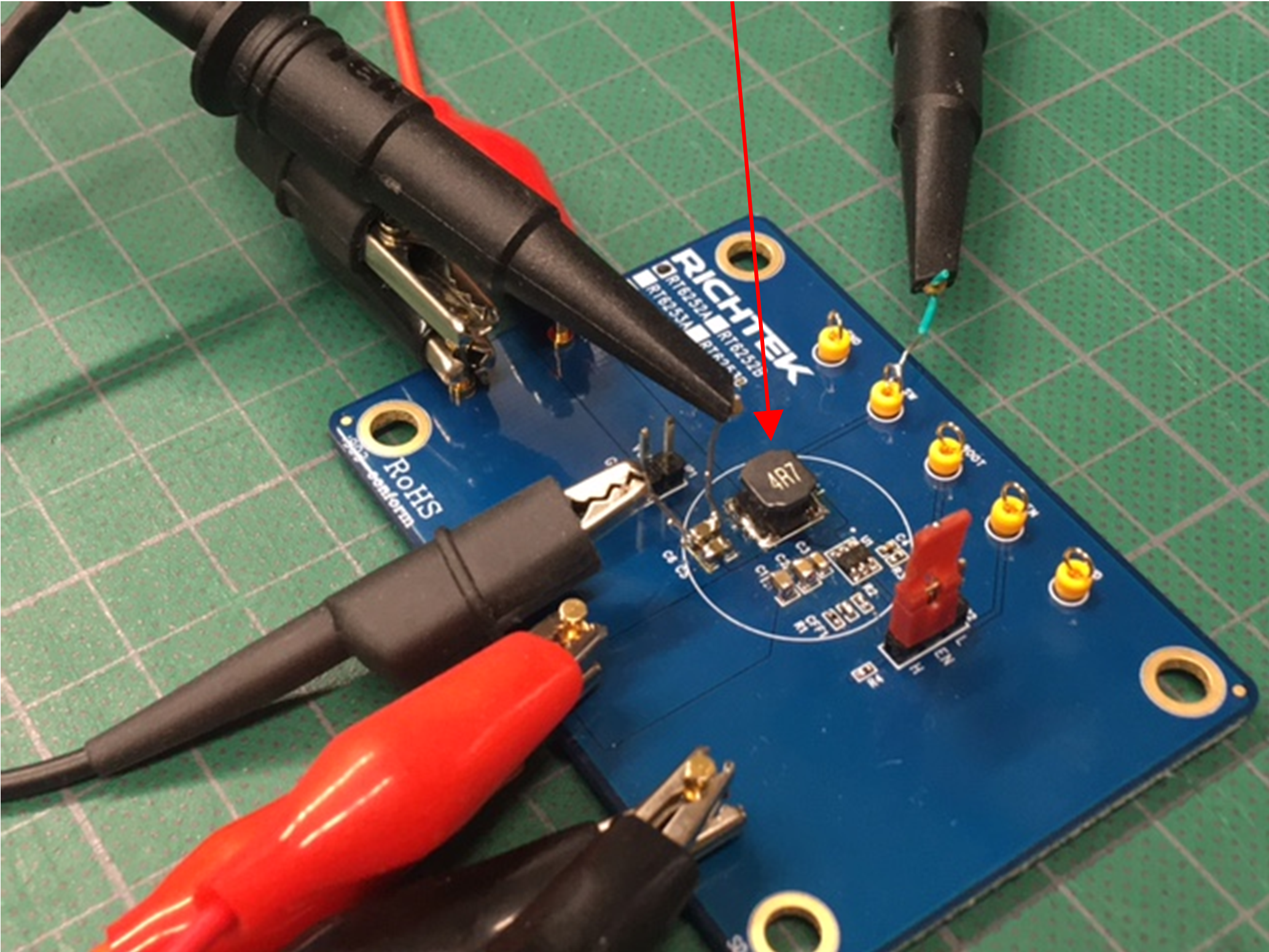
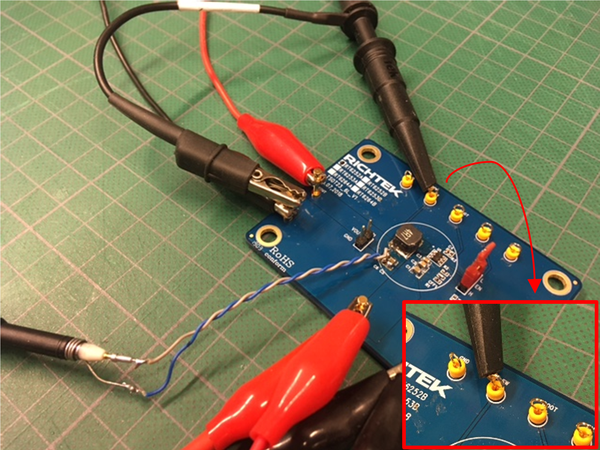
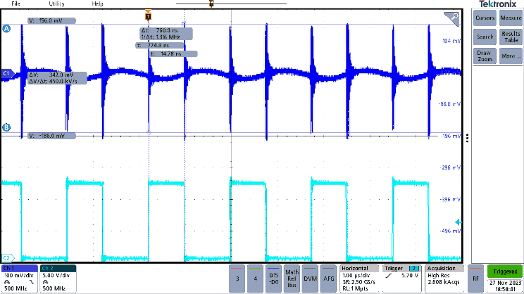
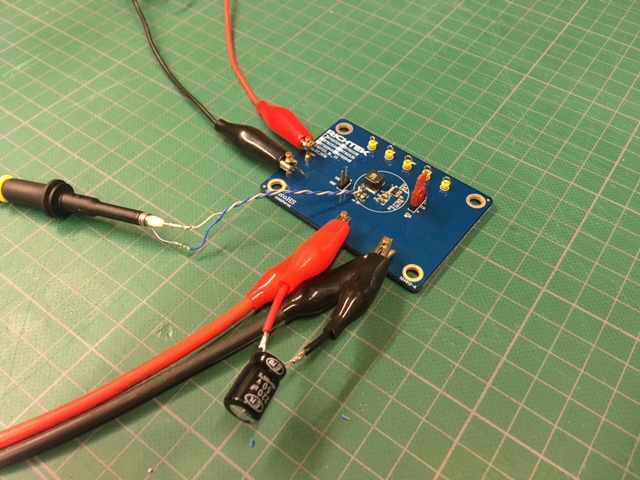
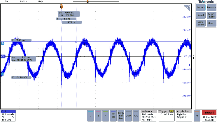
7.1 First measurement setup with large ground loop:
(Figure 16)
We connected a 5Ω (1A) load resistor for CCM operation, and the CH1 probe (yellow ring) with large ground loop to the output capacitor. The CH2 probe (cyan ring) is used to measure the switching waveform with the capacitive pick-up method.
|
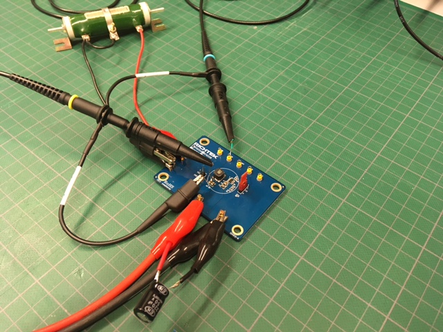
Figure 16
|
A note on inductor orientation in DC-DC converters: SMD inductors are preferably mounted in the orientation where the start of the winding (close to the inner core) is connected to the switching node. In Buck converters, the outer winding will then be connected to the output capacitor node (which has low impedance for high frequencies) and the outer winding thus acts as a shield for the switching signal. This helps improve EMI. When connecting the winding end to the switching node, more high frequency electric field will be emitted by the outer winding area.
When changing the inductor orientation, the stray magnetic field will also be reversed, and this can affect the ripple measurement.
|
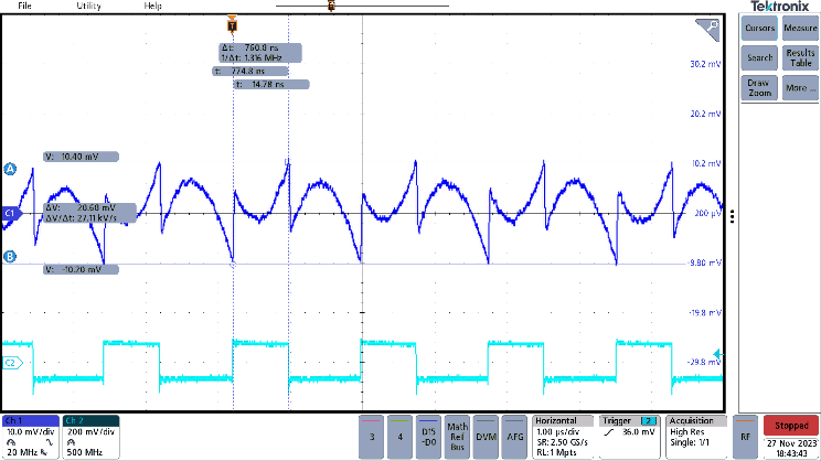
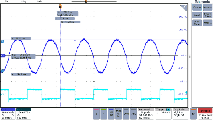
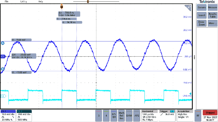
First measurement result (Figure 17)
|
Output ripple measurement (note inductor orientation)
|
Output ripple measurement (reversed inductor orientation)
|
|
|
|
|
Measurement (20MHz BW) with above inductor orientation
|
Measurement (20MHz) with reversed inductor orientation
|
|
|
|
|
Large “negative step” in the measurement
|
Large “positive step” in the measurement
|
Figure 17
It can be seen from the measurements that the CH1 probe in this setup picks up considerable inductor stray field, resulting in large voltage steps in the ripple voltage. There is a big difference in ripple voltage shape when reversing the inductor orientation. The ripple measurements are therefore not accurate.
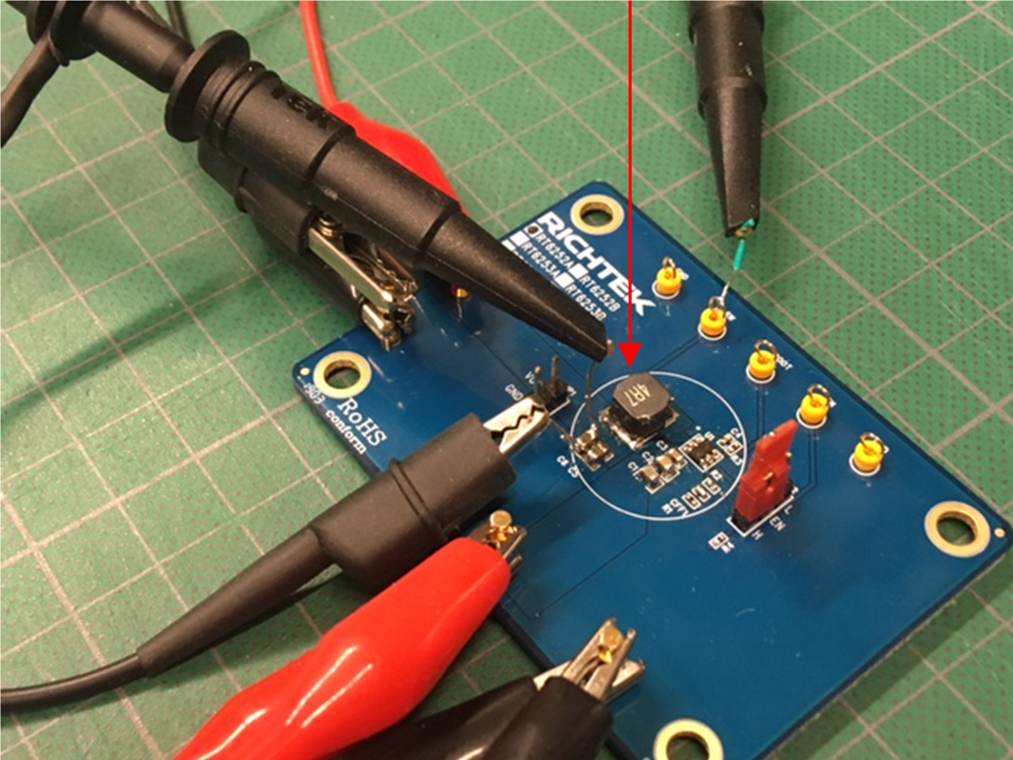
7.2
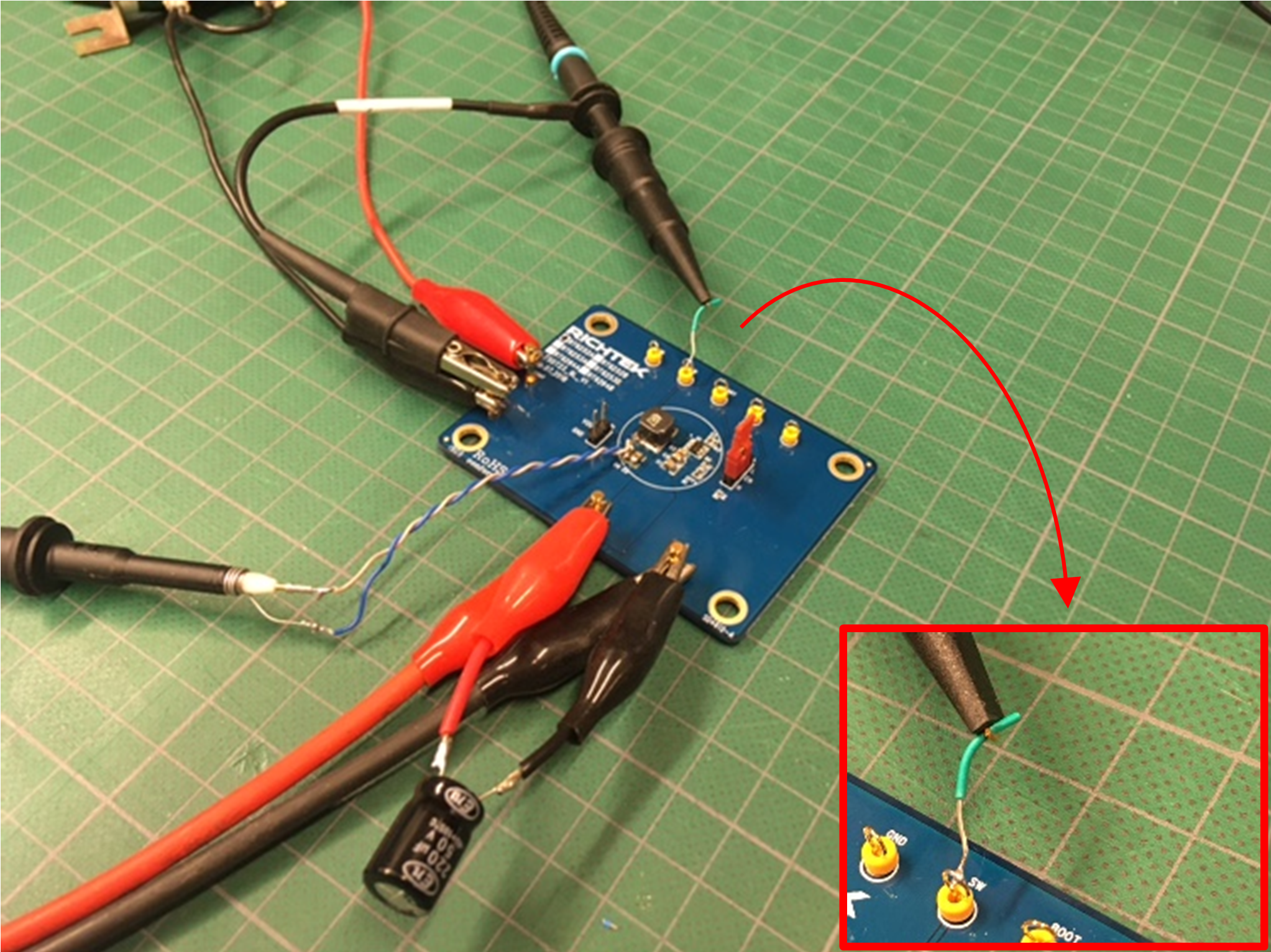
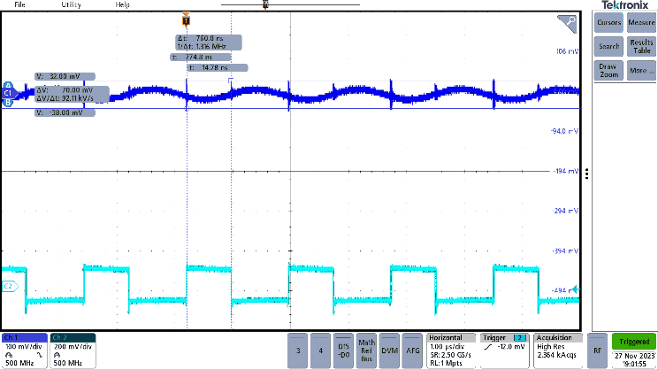
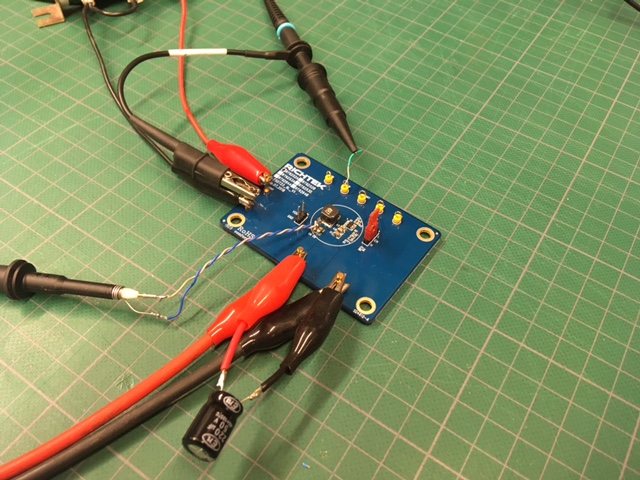
Second measurement setup with small ground loop: (Figure 18)
Here we use the CH1 probe (yellow ring) with shorter ground loop connected to the header for output voltage measurement. The CH2 probe (cyan ring) is used to measure the switching waveform with capacitive pick-up method.
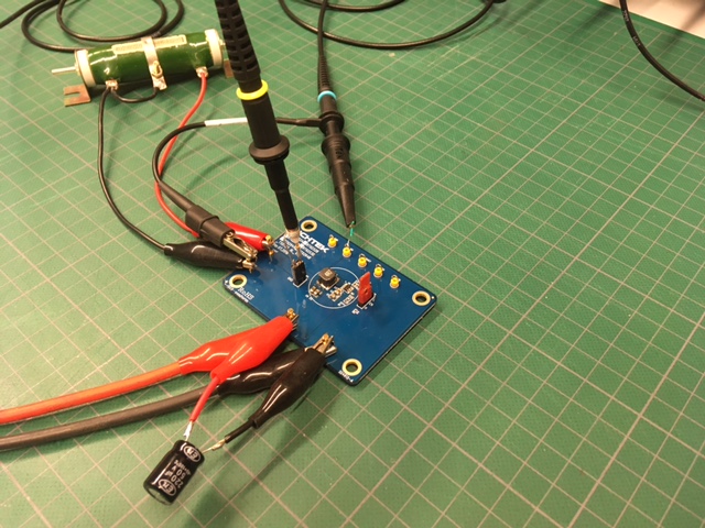
Figure 18
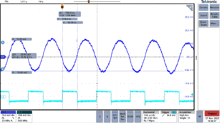
Second measurement result (Figure 19)
|
Output ripple measurement (note inductor orientation)
|
Output ripple measurement (reversed inductor orientation)
|
|
|
|
|
Measurement (20MHz BW) with above inductor orientation
|
Measurement (20MHz) with reversed inductor orientation
|
|
|
|
|
Small “negative step” in the measurement
|
Small “positive step” in the measurement
|
Figure 19
As can be seen from the second measurements, the smaller probe loop picks up much less inductor stray field, but there is still some difference between the two measurements when changing the inductor orientation.
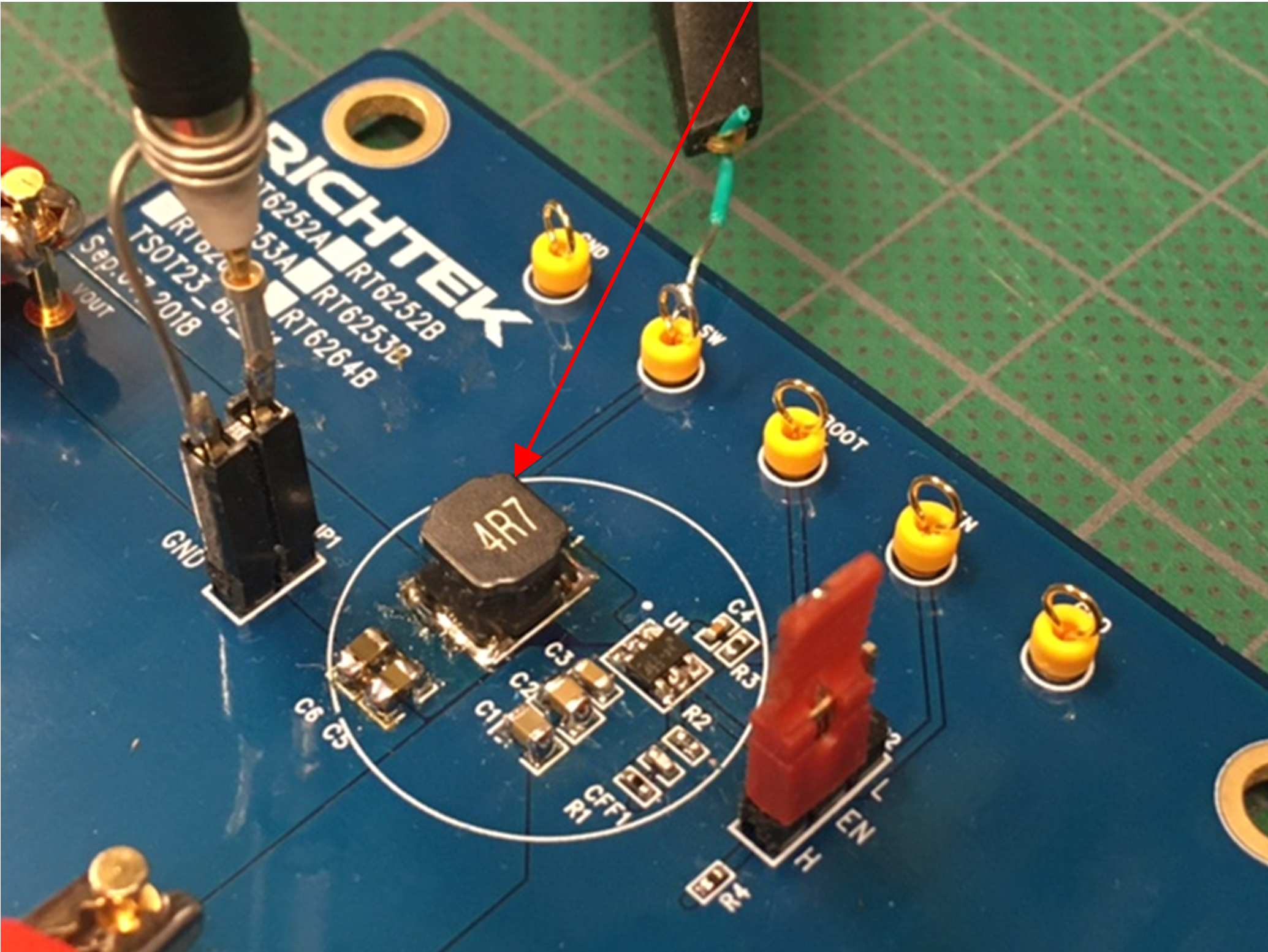
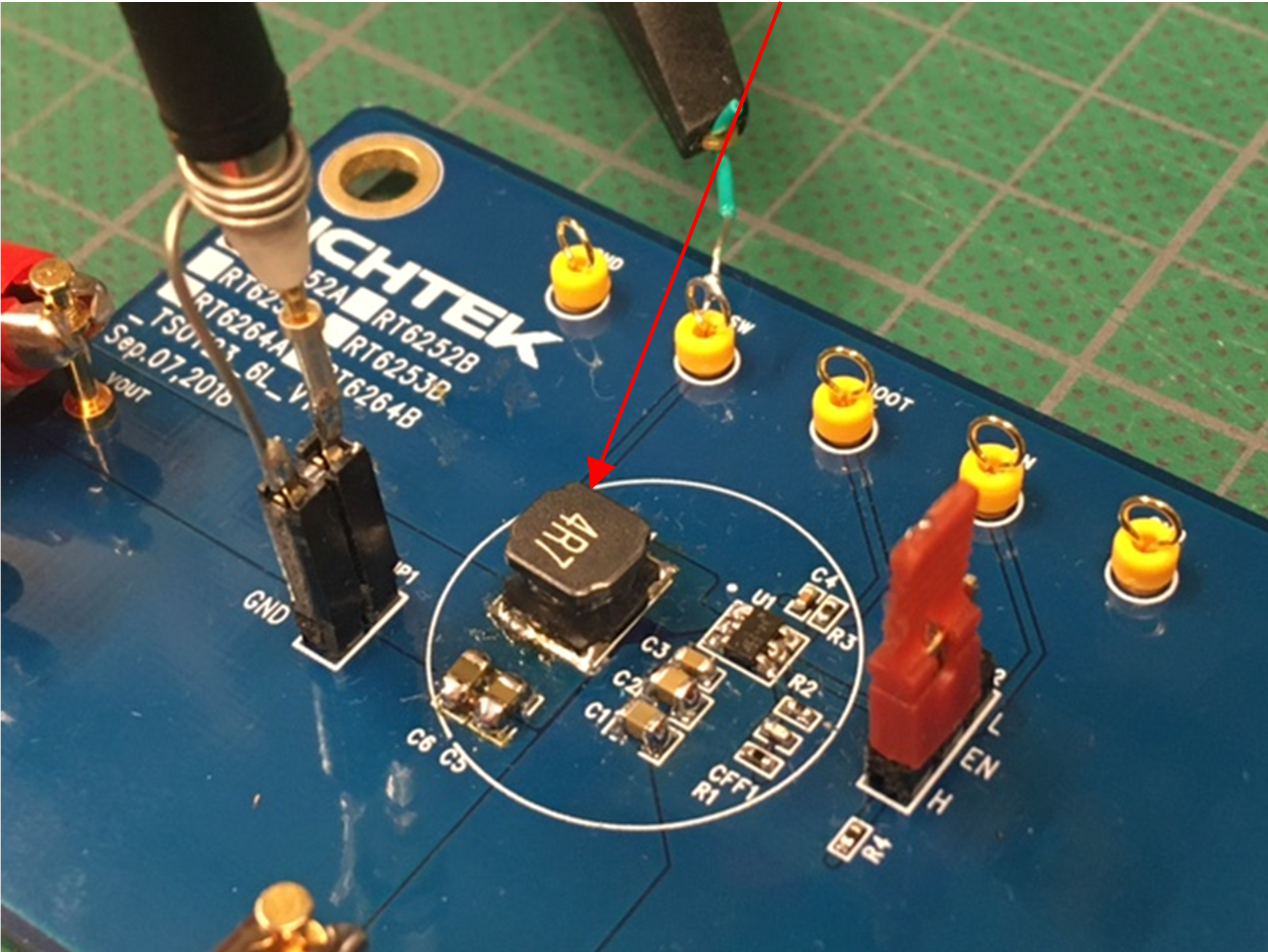
7.3 Third measurement setup with twisted wire: (Figure
20)
Here we connected a twisted wire with very small loop to the output capacitor. The twisted wire loop at the output capacitor was also oriented vertically to minimize inductor stray field pick-up. The CH1 probe (yellow ring) is connected with short ground loop to the other end of the twisted wire, away from the inductor and switching traces. The CH2 probe (cyan ring) is used to measure the switching waveform with capacitive pick-up method.
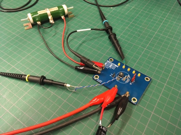
Figure 20
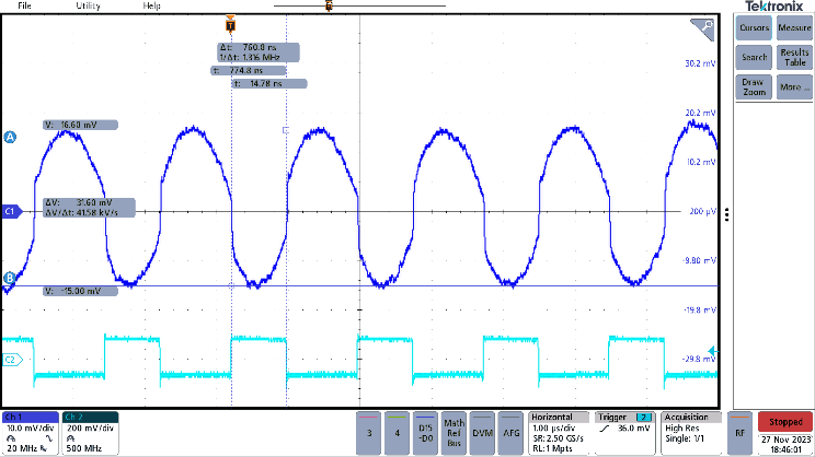
Third measurement result (Figure 21)
|
Output ripple measurement (note inductor orientation)
|
Output ripple measurement (reversed inductor orientation)
|
|
|
|
|
Measurement (20MHz BW) with above inductor orientation
|
Measurement (20MHz) with reversed inductor orientation
|
|
|
|
|
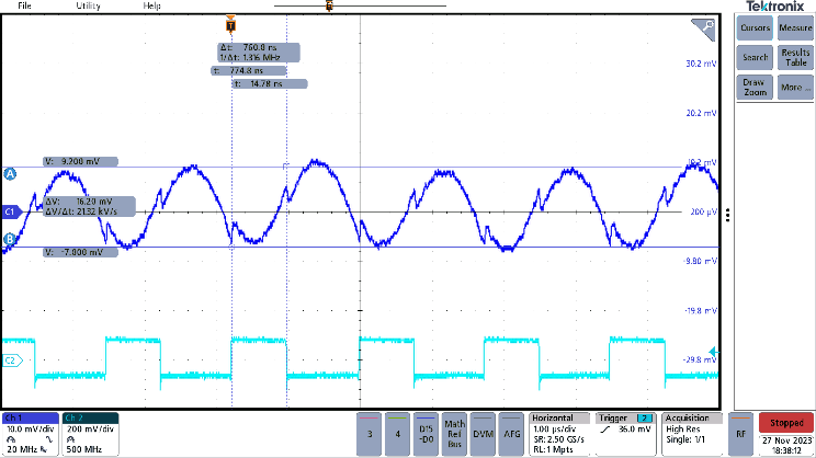
There is hardly any step in the measurement.
|
Hardly any difference when reversing inductor.
|
Figure 21
The twisted wire method shows very clean output ripple measurement, and the fact that the waveforms do not change much when reversing the inductor orientation means that there is hardly any stray field pick-up in the measurement. The CCM ripple measures 22.6Vpp, which is slightly higher than the calculated 18.7mVpp. Note that the ACOT converter has some frequency jitter (OFF-time variation) which causes some irregularities in the measured ripple amplitude.
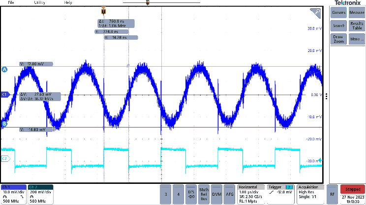
7.4 Measurement with high bandwidth setting (500MHz):
Check the influence of CH2 probe switching signal measurement
Figure 22 shows the difference between direct probe connection and capacitive pick-up method when measuring the switching signal.
|
In below measurement the CH2 probe is directly connected to the switching signal.
|
In the below measurement the CH2 probe is only clamped to the isolation of the wire soldered to the switching signal.
|
|
|
|
|
Measurement (500MHz BW) with direct SW node connection
|
Measurement (500MHz BW) with capacitive pick-up SW connection
|
|
|
|
|
The direct CH2 probe connection adds a lot of HF noise to the ripple voltage measurement
|
CH2 probe with capacitive pick-up of the SW signal hardly adds any noise to the ripple voltage measurement
|
Figure 22
From the measurement comparison, it is clear that the direct probe connection with big ground loop adds a lot of noise to the measurement. Capacitive pick-up method is hardly adding any noise. The amount of capacitive pick-up can be adjusted by changing the distance of the probe clamp related to the inner copper core of the isolated wire.
The best way to measure in high bandwidth setting is to connect as few equipment as possible to the DUT, so only the (resistor) load and only the CH1 probe. (See Figure 23 left side). However, if the switching waveform needs to be viewed (i.e., for scope trigger) the capacitive pick-up method will have low impact on the HF readings.
|
High frequency measurement with only CH1 probe
|
High frequency measurement with CH1 & CH2 probe using capacitive pick-up for the switching waveform measurement
|
|
|
|
|
Measurement (500MHz BW)
|
Measurement (500MHz BW)
|
|
|
|
|
The switching noise in the measurement is relatively small
|
The switching noise in the measurement is relatively small
|
Figure 23
The high frequency spike amplitudes in the above ripple measurements are smaller than the simulation results. Most likely, the very fast (50psec) edges that show in the simulations are attenuated by the 500MHz bandwidth limit of the oscilloscope and probes.
7.5 PSM ripple measurements
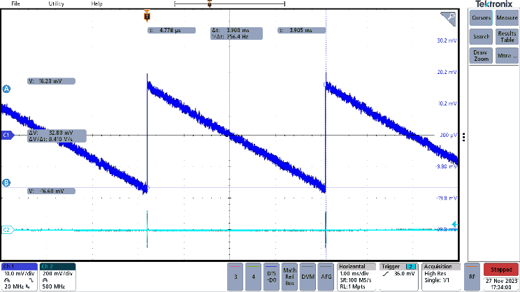
We can remove the resistor load to get low load PSM operation and measure the output ripple in the same way as CCM mode ripple measurement.
We use the twisted wire method for ripple measurement and capacitive pick-up method for switching waveform measurement, see Figure 24.
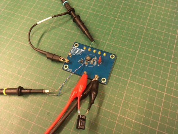
Figure 24
|
Zero load PSM ripple measurement:
|
Detail of PSM switching behavior:
|
|
|
|
|
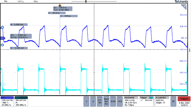
The converter operates at very low frequency: 256Hz
|
The ON time is 510nsec, which is less than the CCM ON time of 750nsec. The PSM ripple amplitude is 32.8mVpp.
|
Figure 25
One of the special features of the RT6252A is that it reduces the ON time in PSM mode, to reduce the PSM ripple amplitude.
The calculated output voltage ripple during PSM mode 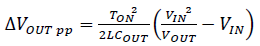 = 33.2mVpp, so the measured ripple of 28.8mVpp matches the calculation result quite well.
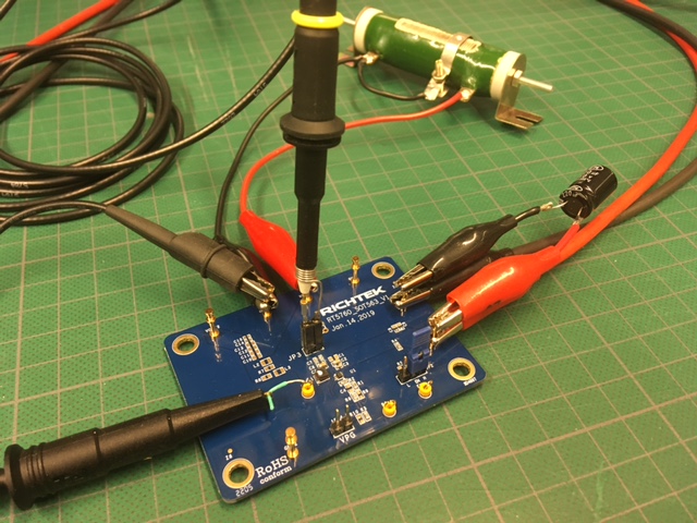
8 Practical example 2: RT5760A ACOT® Buck
converter in 5V to 1.2V, 1A small size & low ripple application
The RT5760A is a cost effective 6V rated 3rd generation low voltage ACOT® buck converter with 1A output current capability and automatic PSM mode at light load. The 2.2MHz switching frequency, SOT563 package and small key components allow for very small size total application footprint. The EVB schematic and layout is shown in Figure 26.
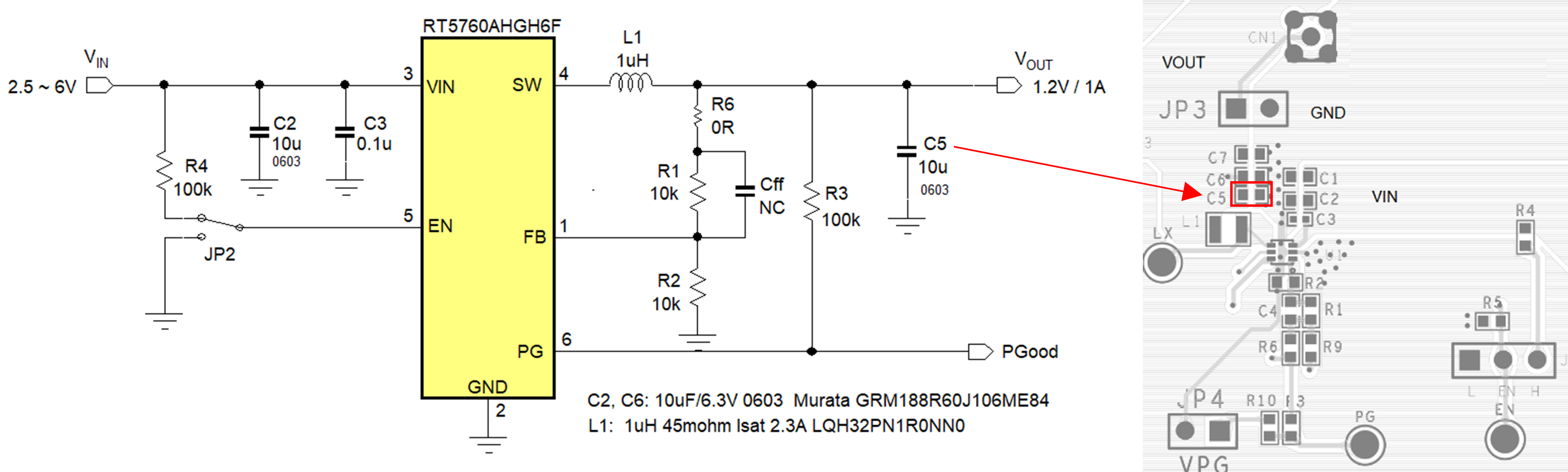
Figure 26
In this small size layout, the single MLCC output capacitor C5 is located very close to the inductor, which is a semi-shielded LQH32 type from Murata. The 10μF/6.3V 0603 MLCC output capacitor drops to 8.6μF at 1.2V DC bias, and at low AC voltage ripple, may drop another 10%. The capacitor has 3mΩ ESR and around 0.2nH ESL (see Figure 27). For this application calculation, we use 8uF effective capacitance, 3mΩ ESR and 0.2nH ESL.
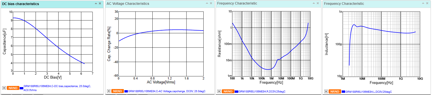
Figure 27
The 1μH 2.3A inductor LQH32PN1R0NN0 has a self-resonance of 150MHz, therefore C-parallel = 1.1pF.
The inductor ripple current 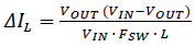 = 0.42App
The output capacitor CCM ripple voltage = 2.94mVpp
The 1.5mΩ ESR, adds  = 1.25mVpp, so total CCM ripple is 4.19mVpp
For the high frequency behavior with parasitic components, below LTSpice simulation shows the results: (Figure 28)
Figure 28
It can be seen that the output waveform is a combination of parabolas (Cout capacitance), triangle (Cout ESR), voltage step (Cout ESL), and the high frequency spikes (caused by inductor parallel capacitance and Cout ESL).
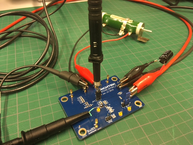
8.1 First measurement with small ground loop:
Figure 29 shows the CCM output ripple measurement: We connected a 2Ω (0.6A) load resistor for CCM operation, and used the short ground loop probe connection and the PCB output voltage header (which is located some distance from the single output capacitor C5) and capacitive pick-up method for switching waveform measurement.
|
Output ripple measurement (10:1 probe)
|
Output ripple measurement (1:1 probe)
|
|
|
|
|
Measurement (20MHz BW) with 10:1 probe
|
Measurement (20MHz) with 1:1 probe
|
|
|
|
|
Due to small ripple, the 10:1 probe sensitivity is not sufficient
|
1:1 probe gives better sensitivity for small ripple measurements.
|
Figure 29
For this very low output voltage ripple measurement, the 10:1 probe does not have sufficient sensitivity. For these kind of low ripple measurements, a 1:1 probe gives better results.
It can also be seen that the short probe loop connection still picks up considerable inductor stray field: The measured waveform (9.1mVpp with large voltage step) is very different from the simulated and calculated (4.2mVpp) result.
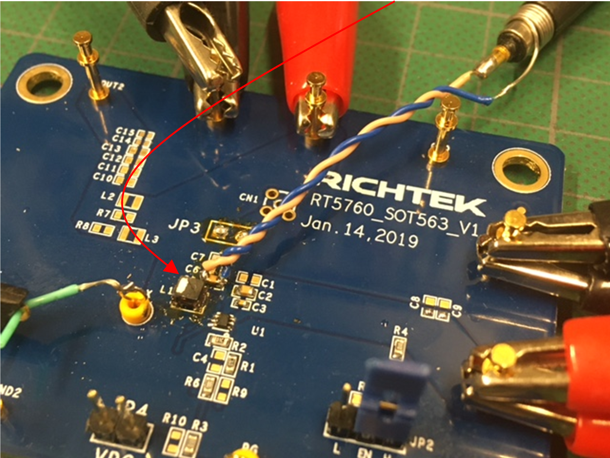
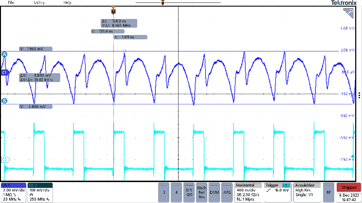
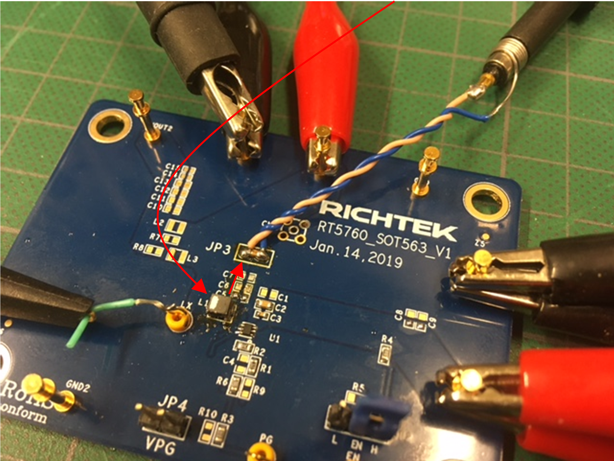
8.2 Second measurement with twisted wire:
Figure 30 shows the output ripple measurement using the 1:1 probe with twisted wire connection directly connected to MLCC output capacitor C5. The twisted wire is connected such that the small loop is vertically orientated to minimize inductor stray-field pick-up.
|
Output ripple measurement (note inductor orientation)
|
Output ripple measurement (reversed inductor orientation)
|
|
|
|
|
Measurement (20MHz BW) (note inductor orientation)
|
Measurement (20MHz) (reversed inductor orientation)
|
|
|
|
|
Measurement does not show any voltage step
|
Measurement still shows considerable voltage step
|
Figure 30
The twisted wire connection has shorter loop than the previous header + short ground loop probe connection, but it can be seen from above measurements that there is still some difference in ripple measurement result when reversing the inductor orientation. Therefore, it is likely that due to the very close proximity of the inductor and the high switching frequency, it is very difficult to avoid some inductor stray-field noise coupled into the small twisted wire.
To reduce the influence of inductor stray field, we can try to move the output capacitor some distance away from the inductor.
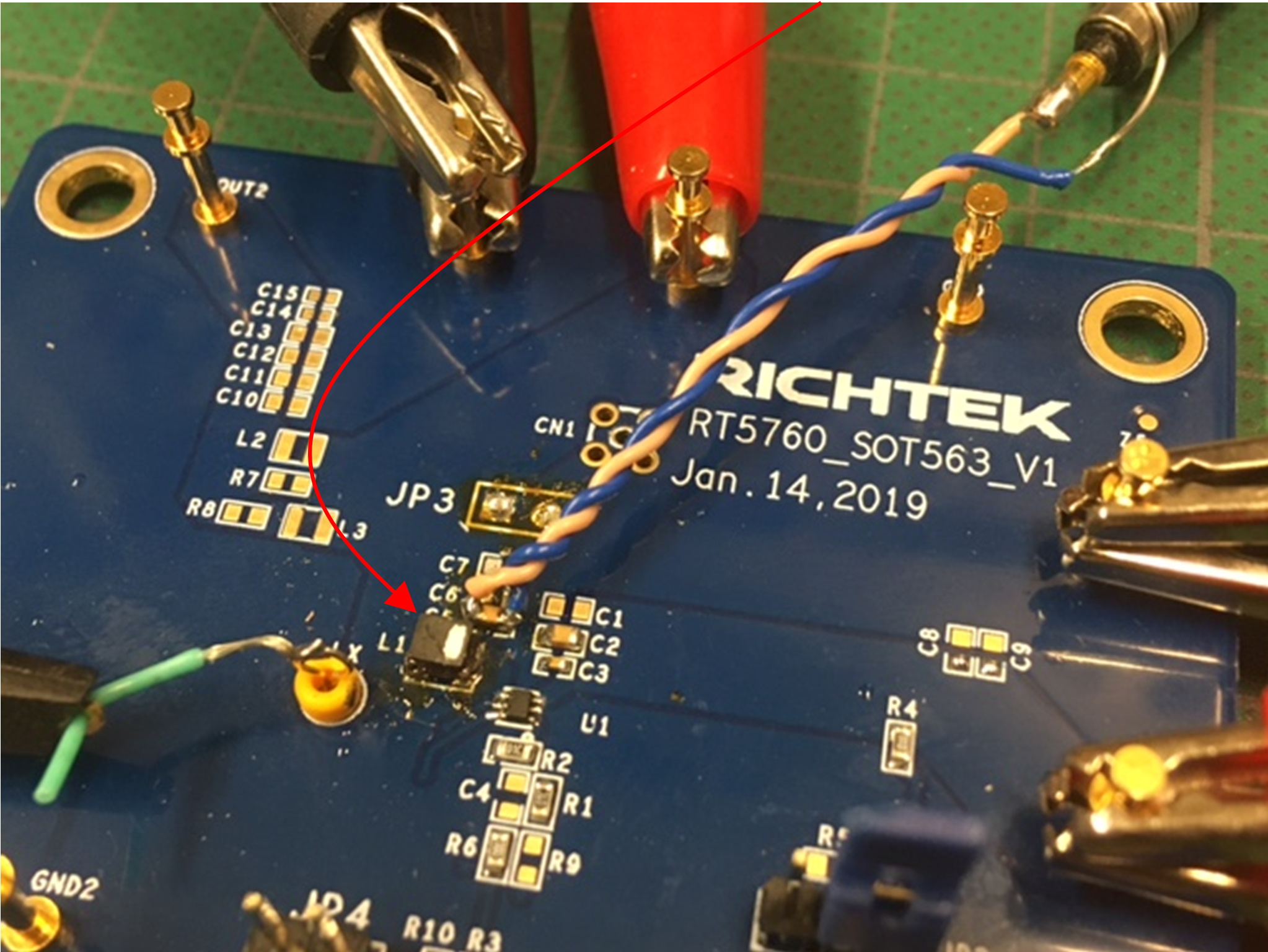
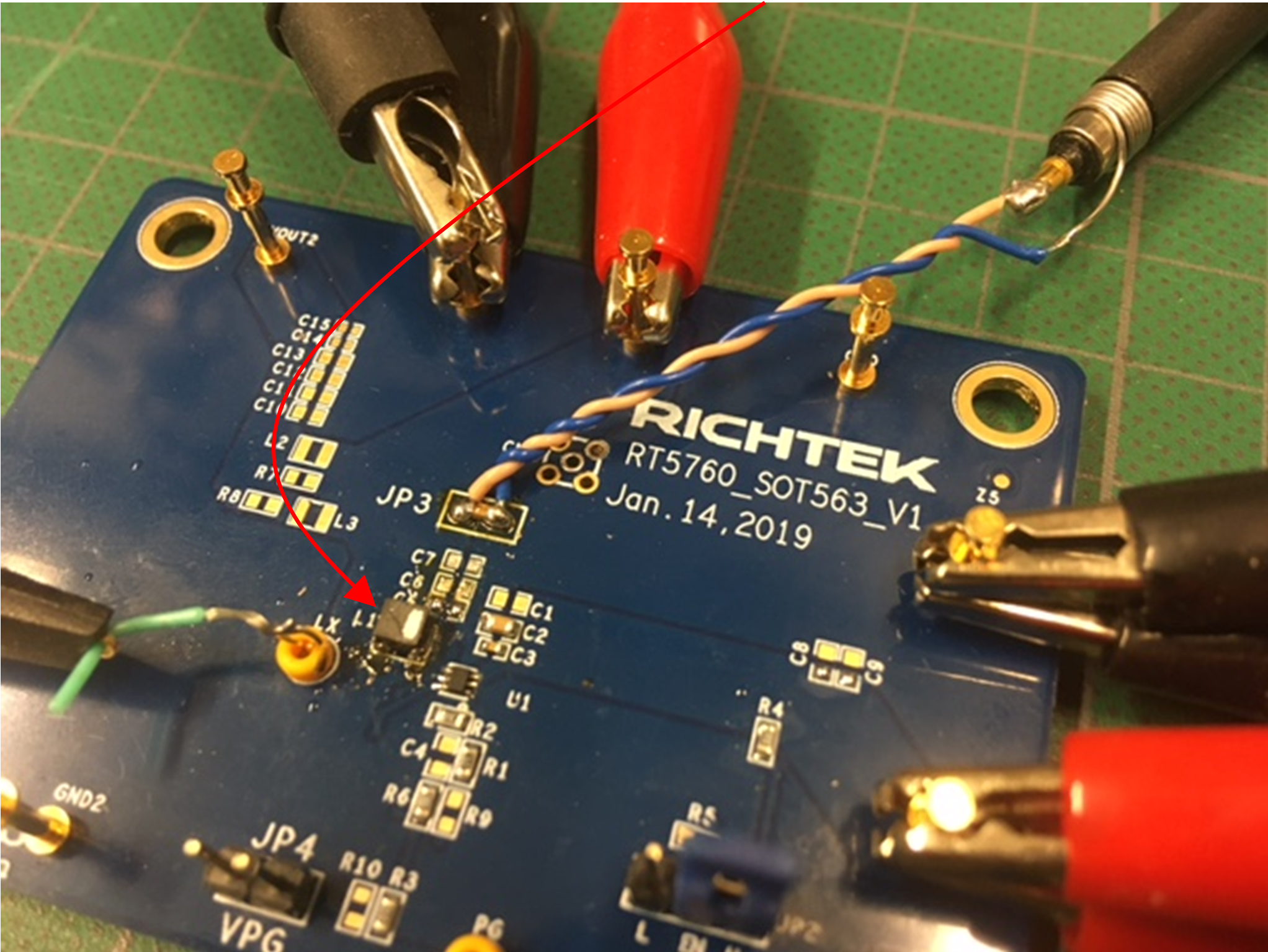
8.3 Third measurement with twisted wire and capacitor
moved away from the inductor:
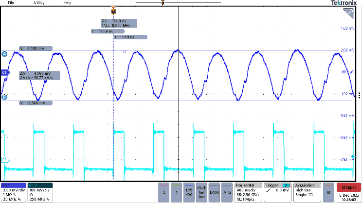
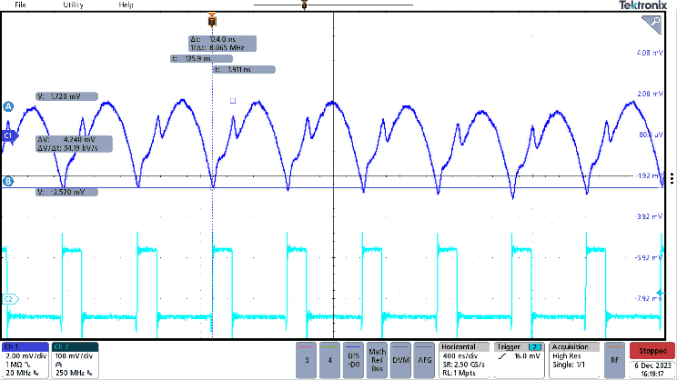
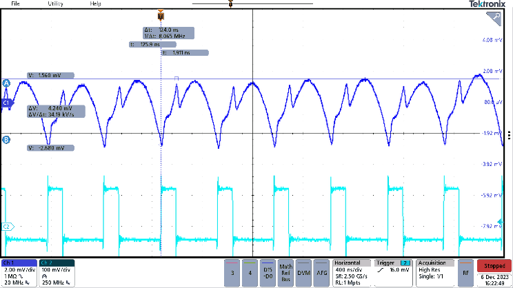
Figure 31 shows the ripple measurement with twisted wire and output capacitor moved 8mm away from the inductor:
|
Output ripple measurement (note inductor orientation)
|
Output ripple measurement (reversed inductor orientation)
|
|
|
|
|
Measurement (20MHz BW) (note inductor orientation)
|
Measurement (20MHz BW) (reversed inductor orientation)
|
|
|
|
|
The measurement shows similar amplitude (4.2mVpp) and waveform shape as the simulated case (4.19mVpp)
|
Very similar waveform shape and amplitude when reversing the inductor orientation.
|
Figure 31
With the twisted wire connection and the output capacitor moved 8mm away from the inductor, the ripple measurement results now match the calculations and simulations with both inductor orientations. Note that the ACOT® converter has some frequency jitter (OFF-time variation) which causes some irregularities in the measured ripple amplitude.
Output ripple measurement with 1:1 probe and 500MHz scope bandwidth setting and capacitive pick-up method for switching waveform measurement). (Figure 32)
|
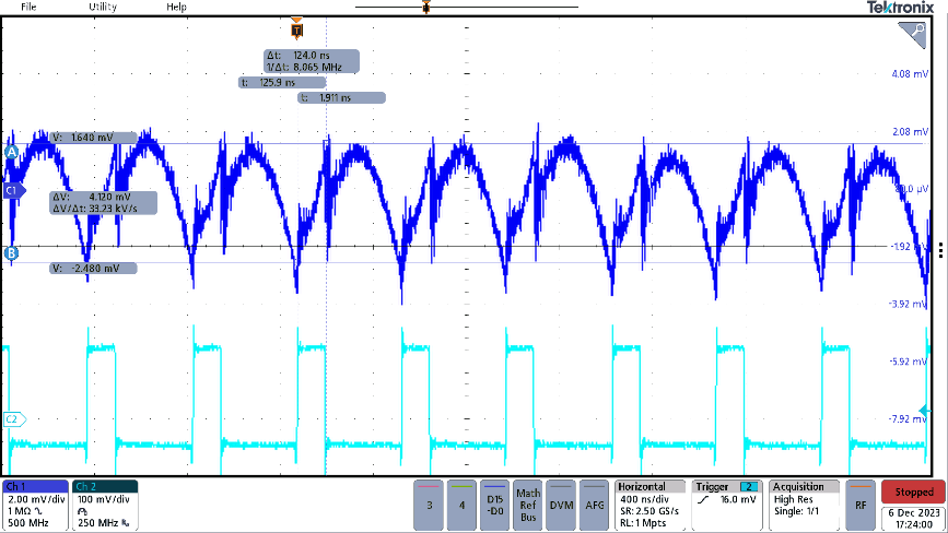
Figure 32
|
It can be seen that with the scope in high bandwidth setting, the measurement does not show much extra high frequency spikes. This is mostly related to the 1:1 probe, which has a useful bandwidth of 15MHz. Most 1:1 probes have relatively low bandwidth, so they are not really capable of showing high frequency signals.
|
8.4 PSM measurement:
For the PSM ripple measurement on the RT5760A EVB, we remove the load resistor and measure the output ripple in the same was as CCM mode ripple measurement (twisted wire method for ripple measurement and capacitive pick-up method for switching waveform measurement), see Figure 33.
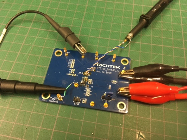
Figure 33
|
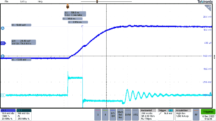
RT5760A zero load PSM ripple measurement:
|
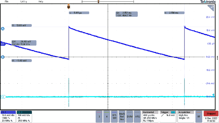
Detail of PSM switching behavior:
|
|
|
|
|
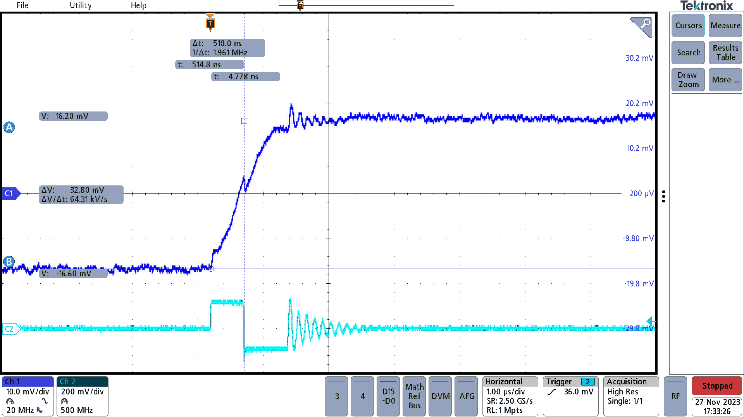
The converter operates at very low frequency: 464Hz
|
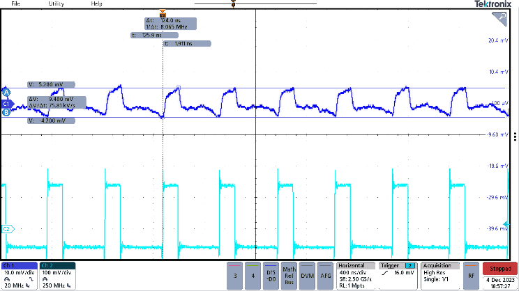
The ON time is 138nsec, which is slightly larger than the CCM ON time of 124nsec. The PSM ripple amplitude is 24.4mVpp.
|
Figure 34
The calculated output voltage ripple during PSM mode  = 29.4mVpp, so the measured ripple of 24.4mVpp is not too far from the calculation result.
9 Tips for DC-DC converter
Gain-Phase measurement setup
Power converter control Loop Gain-phase measurements are normally done by inserting a sinewave sweep signal into the feedback network and measuring the sine wave ripple amplitude and phase at the two sides of the sweep signal insertion point at the output of the converter. (See Figure 35).
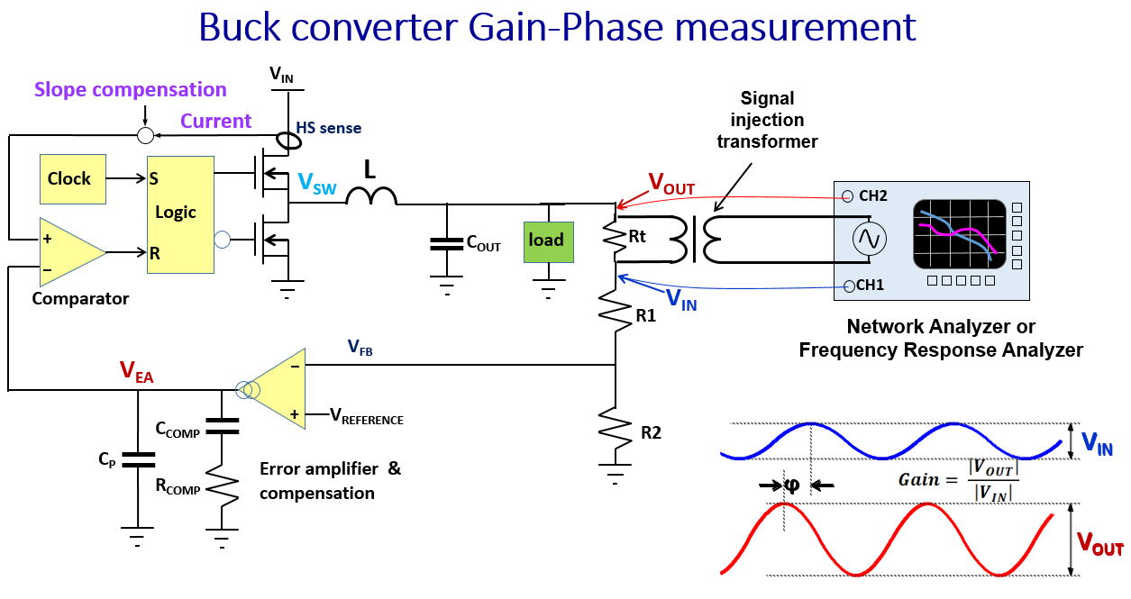
Figure 35
The sine wave sweep signal amplitude must be kept small to avoid changing the operation point of the power converter, and therefore the sine wave signal amplitudes at the measurement points are quite small. For accurate gain-phase measurement results, the measurement should have high sensitivity and the measured signals should have low switching noise. Therefore, the previously discussed output ripple measurement methods can also be applied to gain-phase measurements.
The twisted wire method is very useful when doing gain-phase measurements: the sensitive measurement points can be moved away from the switching converter, and the signal injection transformer leads, CH1 probe and CH2 probe can all be conveniently connected to the twisted wire ends some distance away from the PC board (see Figure 36).
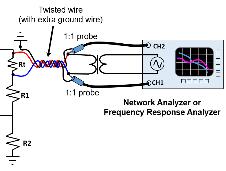
Figure 36
10 Practical gain-phase
measurement example
Figure 37 shows the gain-phase measurement setup for the RT6363GQW 60V/3A buck converter in a 24V to 5V/3A application.
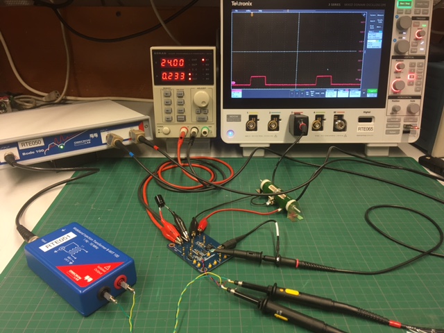
Figure 37
The RT6363GQW is 60V/3A rated current mode buck converter, often used in industrial applications. In this 24V to 5V/3A application, the switching frequency is set at 1MHz, and together with the 24μF effective output capacitance, the external compensation is set for 60kHz crossover frequency. For the gain-phase measurement, a 1.7A resistive load is added to ensure CCM operation. A 4.7Ω resistor is inserted at the top of the feedback network, and the sinewave sweep signal is fed across this resistor. Figure 38 shows the schematic.
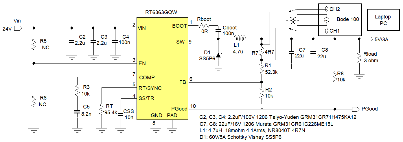
Figure 38
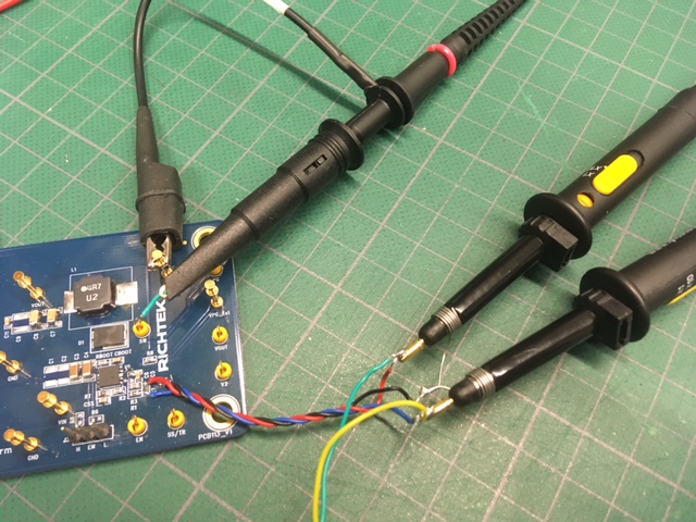
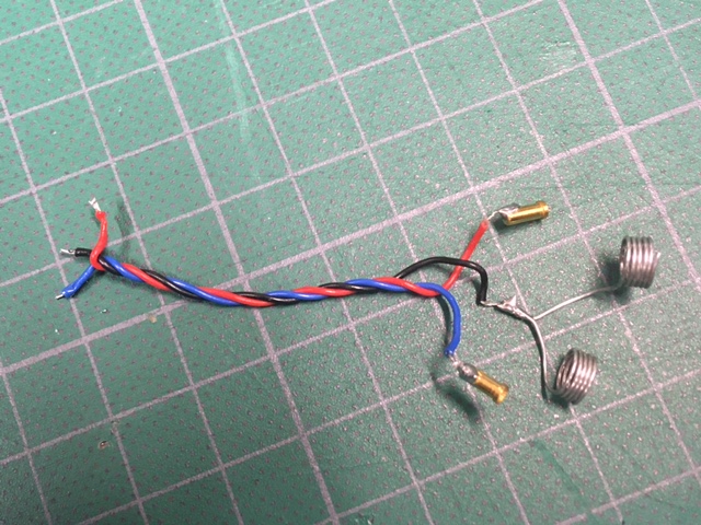
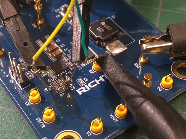
To minimize noise in the measurement, the measurement points at the 4.7Ω resistor are connected to a twisted wire, together with a ground wire, which is connected to a clean small signal ground near the feedback network. The insertion transformer and two 1:1 probes are connected to the other side of the twisted wire. See Figure 39.
|
Detail of the 1:1 probe connections. The switching signal is measured using the capacitive pick-up method.
|
Detail of the twisted wire. The ground is connected to the EVB small signal ground near the feedback network
|
|
|
|
|
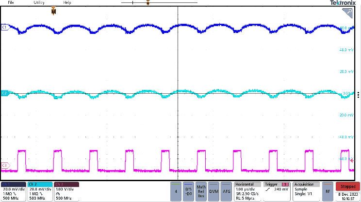
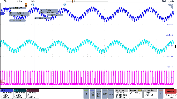
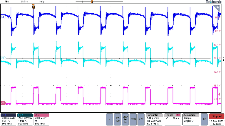
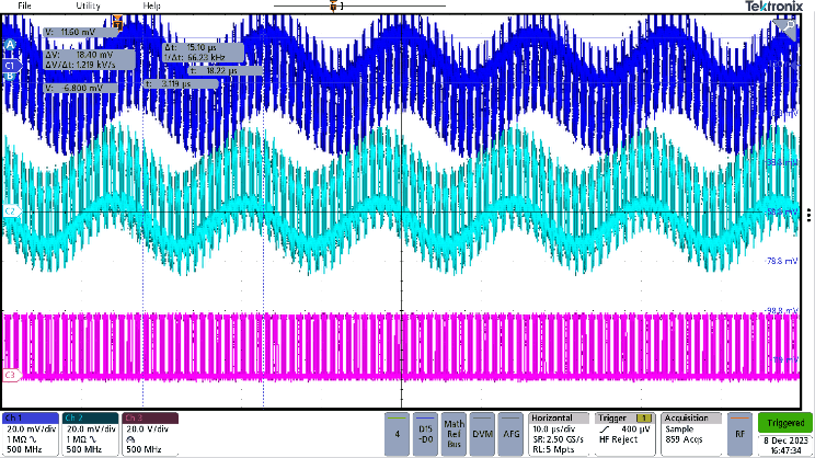
Below are the CH1 and CH2 measurement signals, which have low ripple and very little noise.
|
|
|
|
During the gain-phase sine wave sweep measurement, it is good practice to observe the switching signal duty-cycle variation on the oscilloscope.
|
Figure 39
When doing gain-phase measurements on switching converters, it is important that the insertion sinewave sweep signal is small, to avoid non-linear converter behavior (PSM mode or duty-cycle limiting). In low frequencies, the loop gain is large and insertion signal can also be large to achieve sufficient low frequency sensitivity, but above the converter LC frequency the insertion signal must be small, especially around the cross-over frequency. Most gain-phase analyzers have adjustable insertion signal amplitude.
|
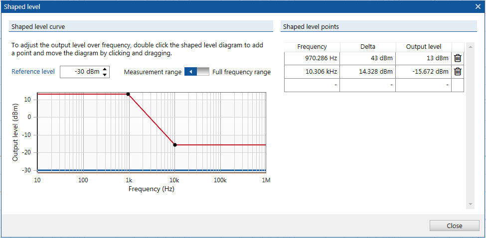
Figure 40
|
Figure 40 shows the BODE-100 analyzer shape level menu. Below 1kHz sweep frequency, the amplitude is maximized, but it must be checked that the insertion transformer does not saturate at low frequency. This can be done by checking for correct sinewave shape.
Above 1kHz the amplitude is reduced. The sine amplitude above 10kHz is set at a fixed low level. The exact amplitude can be checked by observing the switching signal duty-cycle variation around the crossover frequency.
|
|
Below measurement shows the CH1 and CH2 signals with 60kHz insertion signal. The amplitude of the signal will influence the duty-cycle variation in the switching signal. We set 19mVpp insertion signal amplitude. Due to the low noise in the signals, the signal to noise ratio looks OK.
|
Below measurement shows the variation in the duty-cycle with the 19mVpp insertion signal amplitude. The duty cycle variation is small, so there is no risk that the converter would have any non-linear behavior.
|
|
|
|
Figure 41
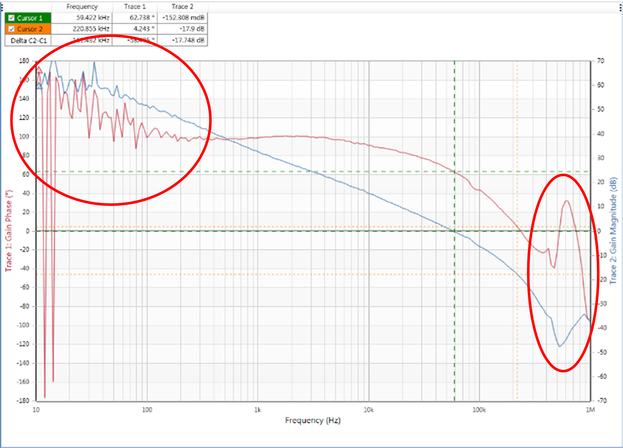
Figure 42 shows the gain-phase measurement result. The curve is smooth and does not show strange behavior. The crossover frequency is 59kHz (close to the 60kHz target value) and the phase margin is 63 degrees.
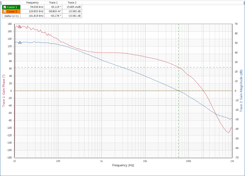
Figure 42
10.1 Second measurement with long ground leads:
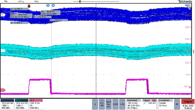
To show what happens when probe connections are used with long ground leads, Figure 43 shows the measurement setup where the CH1 and CH2 1:1 probes are connected with long ground leads and clamps. The switching signal is also measured by connecting the 10:1 probe (with red) ring directly to the switching signal, which adds extra noise.
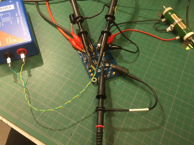
Figure 43
|
Detail of the CH1 and CH2 probe connections to the insertion signal and the CH3 direct connection to the switching signal.
|
The gain-phase measurement now shows more noise in the low frequency range, and there is strange phase behavior in the high frequency range. The BW and PM still look OK.
|
|
|
|
|
Below measurement shows the CH1 and CH2 signals, which contain much more noise than the twisted wire method.
|
The signal to noise ratio at the 60kHz insertion signal setting is bad. It is quite remarkable that the analyzer is still able to get correct gain and phase information from these signals.
|
|
|
|
Figure 44
10 Summary/Practical tips
Minimize the measurement loop
When measuring output voltage ripple for DC-DC converters, the measurement loop area plays an important role in the noise collection. Always try to minimize the probe connection loop area. Using tip and barrel method or twisted wire method can reduce noise pick-up. Check the influence of inductor stray magnetic field by reversing the inductor orientation.
Avoid adding noise to the measurement
Directly connecting probes to fast switching waveforms can add a lot of HF noise. Using very short ground leads or using capacitive pick-up to check the switching signal can minimize the HF noise.
Set the acceptable sampling bandwidth
For different applications, how the critical load is sensitive to the noises, caused by the converter output ripple may vary. For noise-sensitive applications, like high-resolution analog-to-digital converters (ADC) or audio applications, it is recommended to measure output ripple at full bandwidth, while for noise-insensitive applications, the sampling bandwidth of 20MHz may be chosen. Note that background noises still need to be checked at the full oscilloscope sampling bandwidth, so that the output ripple may not be measured inaccurately.
Check signals in time domain before running gain-phase analysis.
In Gain-Phase measurements, always check the measured signals on the oscilloscope before connecting them to the Frequency Response Analyzer. Minimize noise in the signals for best results.
For a practical example video of loop gain-phase measurement, see https://www.youtube.com/watch?v=YHCQ0GDlw6Q
To stay updated with more information about our products, please subscribe to our newsletter.